Bluetooth Smart is a popular choice for the wireless control of the latest indoor LED lamps. With Bluetooth connectivity included in every smartphone and tablet, a ready-made interface provides the user with simple set-up and control of a lamp.
Using a smartphone gives the system designer many more options for implementing new features in a lamp, such as changing the balance of colors or the quality of the light.
Such control can be achieved with the combination of the SimpleLink™ CC2540T high temperature wireless transceiver and controller from Texas Instruments coupled with the TPS76933 voltage regulator and the TPS62290 DC-DC converter to power the actual LEDs in the lamp. Low power consumption is not a direct concern, as the LED lamps are often powered from a mains supply, but a low-power design means a lower operating temperature and higher reliability, giving the lamp a longer lifetime.
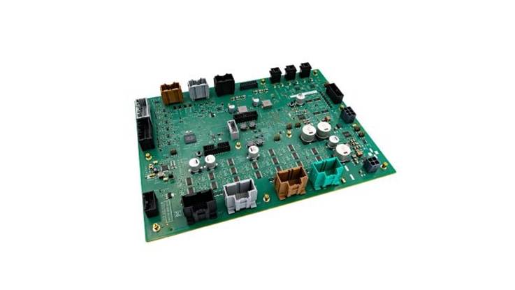
A USB-based demonstration system includes a fully tested design with firmware, GUI, demo and getting started guide, and a full bill-of-materials.
The heart of the design is the CC2540T, which is packaged in a compact 6 x 6 mm 40-pin quad flat pack. This is a cost-effective, low-power, true wireless MCU for Bluetooth low energy applications based around an 8051 microcontroller core. The device enables a robust BLE master or slave node to be built with a very low total bill-of-materials by integrating in-system programmable flash memory, 8 KB of RAM, and other powerful supporting features and peripherals. The CC2540T is suitable for systems where very low power consumption is required as very low-power sleep modes are available. A short transition time between operating modes further enables low power consumption.

Figure 1: The SimpleLink CC2540T combines a 2.4 GHz radio front end with an 8051 controller running a full Bluetooth stack.
The BLE Light demonstration boards are powered through the USB connector using a dedicated USB power supply capable of supplying at least 800 mA and max 5.5 V. A similar supply can be used for the VDD supply to pins 2 and 3 in Figure 2.
The transceiver uses a 32 MHz crystal oscillator on pins 22 and 23 (XOSC_Q1andQ2) to provide the internal 8 MHz clock, and is connected to a simple 2.4 GHz dipole antenna via a bandpass filter on pins 25 and 26 (RF_P and RF_N).
The design in Figure 2 shows how the output of the controller at P0_3 to 6 is used to control four LEDs. With power from the 3.3 V output of a DC-DC converter (see below), the control signals provide the switching and balance for each device. From a custom app running on a smartphone (provided in the reference design), this allows the user to create a particular color balance and intensity.

Figure 2: The LED lighting reference design connects up the CC2540T Bluetooth transceiver and controller with a voltage regulator and DC-DC converter to power the LEDs.
The design uses the TPS62290 DC-DC step down converter. This provides the 3.3 V power to the LEDs from VDD. An automotive-qualified part provides temperature specification up to 105°C to match the high temperature operation of the CC2540T transceiver. This allows the transceiver and DC-DC converter to be placed closer to the LED in the end design.
The TPS62290 operates with a 2.25 MHz fixed frequency pulse-width modulation (PWM) at moderate to heavy load currents. At light load currents, the converter can automatically enter Power Save Mode and then operate in PFM mode. During PWM operation, the converter uses a unique fast-response voltage mode controller scheme with input voltage feedforward to achieve good line and load regulation, allowing the use of small ceramic input and output capacitors.
At the beginning of each clock cycle, the high-side MOSFET switch is turned on. The current flows now from the input capacitor through the high-side MOSFET switch through the inductor to the output capacitor and load. During this phase, the current ramps up until the PWM comparator trips and the control logic turns off the switch. The current limit comparator also turns off the switch if the current limit of the high-side MOSFET switch is exceeded.
After a dead time preventing shoot-through current, the low-side MOSFET rectifier is turned on, and the inductor current ramps down. The current flows now from the inductor to the output capacitor and to the load. It returns to the inductor through the low-side MOSFET rectifier. The next cycle is initiated by the clock signal again turning off the low-side MOSFET rectifier and turning on the high-side MOSFET switch.
The TPS76933 low-dropout (LDO) voltage regulator provides a low dropout voltage, ultra-low-power operation and miniature packaging to fit into an LED lamp by using a 5-terminal small outline integrated circuit SOT-23 package.
The design replaces the usual PNP pass transistor with a PMOS pass element which acts as a low value resistor so the dropout voltage is very low, typically 71 mV at 100 mA of load current and is directly proportional. As the PMOS pass element is voltage driven, the quiescent current is as low as 28 µA and is stable over the range of output load current from 0 mA to 100 mA.
Software
The software supplied with the reference design provides the Bluetooth v4.0 Compliant Protocol Stack for a Single-Mode Bluetooth Low Energy (BLE) implementation with a complete stack optimized for low power, including the controller and host. The GAP profile software includes central, peripheral, observer or broadcaster modes, including combination roles, so that an LED lamp can broadcast its identity and capability to a phone, and the application can run on the CC2540T without an external controller. The stack also supports AES-128 encryption and decryption to keep the devices secure, making use of a unique 48-bit IEEE identifier in each chip and a security co-processor.
The profiles are accessed by a high-level iOS or Android application running on a smartphone that controls the colors, brightness and combination of the LED lamps as in Figure 3. This can also provide other features such as the signal strength to the Bluetooth transceiver and the lamps being addressed by the smartphone in a group as shown in Figure 4.

Figure 3: The controller app running on a smartphone.

Figure 4: The additional features on the app.
A Windows PC application is available for evaluation and development, as well as running the CC2540TDK-LIGHT development tool that uses the JTAG port shown in the schematic in Figure 2. The software, schematics and design guide can be downloaded from the TI website.
Conclusion
The combination of the CC2540T 2.4 GHz transceiver, TPS62290 DC-DC converter and the TPS76933 LDO regulator provides a high temperature, low power implementation for the wireless control of an LED lamp. Low power operation reduces the temperature of operation and enhances the reliability and lifetime of the lamp. The high level of integration allows the components to be designed into a smaller area, creating a less bulky LED lamp. The output of the CC2540 Bluetooth transceiver can directly control the LEDs in the lamp, allowing an app on a smartphone to create a wide range of different color temperatures and intensities. Additional features such as RSSI signal strength are measured to enable the developer to evaluate the performance of the wireless link in operation.


