This article looks at how ultra-low-power wireless transceivers in the sub 1 GHz bands and the KNX protocol can be used to implement self-powered networks in the smart home, using either energy harvesting or long-life batteries for applications such as lighting and monitoring.
An emerging standard for low-cost wireless networking in the smart home is opening up opportunities for innovative designs. With the latest wireless transceivers and microcontrollers, ultra-low-power designs that can be powered directly by solar panels through energy harvesting can be developed.
Rather than using a single chip with a 2.4 GHz transceiver, developers are looking at lower-cost, lower-power transceivers in the ISM band of 240–960 MHz coupled with 8- or 16-bit ultra-low-power microcontrollers and the new protocol. The lower frequency gives longer range and lower power consumption, while the KNX protocol is optimized for smart home devices with a focus on lower power, opening up the opportunity for self-powered devices and hubs.
The KNX protocol is currently used in over 70% of European smart-home devices, addressing a market estimated at over €600 million in Europe alone. As an open standard, KNX promotes interoperability, saves costs, and enhances flexibility for product developers and equipment owners. Now managed by the KNX Association, it is ratified as CENELEC EN 50090 or CEN EN 13321-1 in Europe, GB/Z 20965 in China, ANSI/ASHRAE 135 in the USA, and globally as ISO/IEC 14543-3.
The focus of the KNX standard (formerly EIB/Konnex) is home and building control. The most typical application areas are lighting, shutters, or heating and cooling. The standard covers the wired-media twisted pair, power line, and Ethernet. In locations not suitable for cabling, KNX-RF is used for wireless data transmission within a building. As the complete KNX standard, the wireless part KNX-RF is vendor independent, allowing a range of RF transceivers to be used alongside different microcontrollers. This is opening up opportunities for ultra-low-power designs.
The KNX Advanced Interface (KAI) is the main software component of KAI and provides the complete functionality needed for KNX devices. This contains all elements required by the KNX standard and is certified in several different configurations. KAI maps closely to the ISO/OSI reference model with a clear structure that separates between application-relevant parts, modular communication stack internal parts, media-dependent parts, and target-CPU related issues (Figure 1). Advanced implementation methods allow highly-efficient coding that leads to optimized resource usage. This is shown in a small footprint and the moderate resources needed. An application development with KAI relieves the burden of early decisions in the design process by simple configurability of the stack.

Figure 1: The KNX Advanced Interface (KAI) reference model.
It helps increase system reliability and improves device stability. Hardware and software components of KAI can be adapted according to given conditions.
Addressing scheme
The addressing scheme is based on the system architecture used for twisted pair, which uses individual and group addresses (each with two bytes). The individual address is a single-cast address and is mainly used for configuration purposes. Group addresses are used for runtime communication and 0x0000 is reserved as the broadcast address.
As RF is an open medium like power line, a domain address (six byte, programmable) has been added to allow for separate but neighboring installations, and as unidirectional devices cannot be programmed, they cannot use an installation-specific domain address. Instead, group telegrams contain the serial number of the sender, and the serial number together with the 2 byte group address is called an extended group address.
This has implications for the design of the wireless hub.
Hub design
The CC1120 from Texas Instruments is an integrated ISM band transceiver that can be used with a microcontroller such as the MSP430F2370 to implement a bidirectional KNX low-power radio link for a low-power hub.

Figure 2: The TI CC1120 low-power ISM band transceiver.
The CC1120 can be configured via a simple 4-wire SPI-compatible interface (SI, SO, SCLK and CSn) where the RF chip is the slave. All address and data transfer on the SPI interface is done with the most significant bit first, and all the transactions on the SPI interface start with a header byte containing a read/write bit, a burst access bit, and a 6-bit address. During address and data transfer, the CSn pin (Chip Select, active low) must be kept low.
The 4-wire interface could be connected to an on-chip USART in synchronous mode, configured as master, but for most applications it is more useful to realize this interface via standard I/O pins and to save the USART for the data interface.
The transceiver includes a packet handler, but because of the different structure of the KNX-RF frames, this cannot be used. This means the chip has to be used in synchronous serial operation with the complete packet coding and decoding (using inclusive Manchester code) handled in the microcontroller.

Figure 3: Connecting the CC1120 transceiver to an MSP430 microcontroller to implement KNX.
As the CC1120 has to be used in NRZ mode, the microcontroller has to send and receive the data bits in real-time. To save calculation power it is recommended to use a USART in synchronous mode for sending and receiving. This is especially important for bidirectional devices. Send-only devices may use only standard I/O pins for communications; so even a microcontroller without integrated USART might be used.
When using the USART at a chip rate of 32,768 cps specified for the KNX protocol, 4,096 patterns per second must be evaluated or sent. In receive mode the patterns sampled by the USART are not synchronized, so the software permanently has to scan for the start of frame.
The transceiver requires its own crystal to generate the radio frequency and the bit timing, so the timing of the physical layer is completely controlled by the radio chip. To comply with the KNX Standard, an overall accuracy of ±35 ppm must be achieved.
If there is no requirement for precise timing for the application task, the MSP430 can be clocked using DCO frequency. The required frequency depends on the type of connection to the RF chip (HW or SW UART) and on software efficiency.
A key element of the CC1120 is a fully-integrated, fractional-N, ultra-high-performance frequency synthesizer that is designed for excellent phase noise performance, providing very-high selectivity and blocking performance. The system is designed to comply with the most stringent regulatory spectral masks at maximum transmit power.
Either a crystal can be connected to XOSC_Q1 and XOSC_Q2, or a TCXO can be connected to the EXT_XOSC input. The oscillator generates the reference frequency for the synthesizer, as well as clocks for the ADC and the digital part. To reduce system cost, the CC1120 has high accuracy-frequency estimation and compensation registers to measure and compensate for crystal inaccuracies, enabling the use of lower-cost crystals. If a TCXO is used, the CC1120 will automatically turn the TCXO on and off when needed to support low-power modes and Wake-On Radio operation.
The CC1120 also features a highly-flexible receiver. The received RF signal is amplified by the low-noise amplifier (LNA) and down-converted in quadrature (I and Q) to the intermediate frequency (IF). At the IF, the I/Q signals are digitized by the high dynamic-range ADCs. An advanced Automatic Gain Control (AGC) unit adjusts the front-end gain, and enables the CC1120 to receive both strong and weak signals, even in the presence of strong interferers. This helps the network link work more effectively across the home. High attenuation-channel and data filtering enable reception with strong neighbor-channel interferers.

Figure 4: The TI KNX development board showing the small size possible for smart-home network implementations.
The I/Q signal is converted to a phase/magnitude signal to support both FSK and OOK modulation schemes, and a sophisticated pattern-recognition algorithm locks onto the synchronization word without the need for preamble settling bytes. Receiver settling time is therefore reduced to the settling time of the AGC, which is typically 4 bits. This helps to speed up the link process and keep power consumption to a minimum.
The advanced pattern recognition also greatly reduces the problem of false sync triggering on noise, further reducing power consumption and improving sensitivity and reliability. This is also important in preventing false signals in the home network, which has to be reliable with minimal power consumption.
A novel I/Q compensation algorithm removes any problem of I/Q mismatch, and hence avoids time consuming and costly I/Q image calibration steps in production or in the field.
The transmitter is based on direct synthesis of the RF frequency (in-loop modulation). To achieve effective spectrum usage, the CC1120 has extensive data filtering and shaping in TX to support high throughput data communication in narrowband channels. The modulator also controls power ramping to remove issues such as spectral splattering when driving external high-power RF amplifiers.
Radio control and user interface
The CC1120 digital control system is built around MARC (Main Radio Control) implemented using an internal high-performance 16-bit ultra-low-power processor. This handles power modes, radio sequencing, and protocol timing.
A 4-wire SPI serial interface is used for the configuration and data buffer access. The digital baseband includes support for channel configuration, packet handling, and data buffering. The host MCU can stay in power down until a valid RF packet has been received, and then burst read the data, greatly reducing the power consumption and computing power required from the host MCU.
The CC1120 radio control and user interface is based on the widely-used CC1101 transceiver to enable easy SW transition between the two platforms. The command strobes and the main radio states are the same for the two platforms.
The Enhanced Wake-On-Radio (eWOR) uses a flexible integrated sleep timer that enables automatic receiver polling with no intervention from the MCU. The CC1120 will enter receive mode, listen and return to sleep if a valid RF packet is not received. The sleep interval and duty cycle can be configured to make a trade-off between network latency and power consumption. Incoming messages are time-stamped to simplify timer re-synchronization.
The eWOR timer runs off an ultra-low-power 32 kHz RC oscillator. To improve timing accuracy, this can be automatically calibrated to the RF crystal in configurable intervals.
The CC1120 also uses eWOR to support very-quick start-up times, and requires very few preamble bits, again saving power. Sniff Mode uses this to dramatically reduce the current consumption while the receiver is waiting for data. As the CC1120 is able to wake up and settle much faster than the length of most preambles, it is not required to be in receive mode continuously while waiting for a packet to arrive. Instead, the enhanced wake-on-radio feature can be used to put the device into sleep periodically. By setting an appropriate sleep time, the CC1120 will be able to wake up and receive the packet when it arrives with no performance loss. This removes the need for accurate timing synchronization between the transmitter and receiver, and allows the user to trade off current consumption between the transmitter and receiver.
According to the KNX-RF standard, a stack implementation has to differentiate between unidirectional and bidirectional devices. Unidirectional devices contain only the send function and a highly-simplified communication stack. The software supports a power-save mode to lengthen battery life. Because the unidirectional software has a code size of only a few kBytes, very inexpensive controllers can be used.
A bidirectional implementation has both a sender and a receiver. Although processing of received data is time-critical due to the relatively high data rate, it is still possible to detect and correct individual bit errors during reception. Consequently, communication quality is very high even when transmission conditions are unfavorable. Bidirectional devices require a complete communication stack that also includes the link mechanism for putting the device into operation.
STM8
Other microcontrollers such as the STM8 family from STMicroelectronics can also be used to run the KNX stack. The STM8L101xx low-power family features the enhanced STM8 CPU core, providing increased processing power (up to 16 MIPS at 16 MHz) while maintaining the advantages of CISC architecture with improved code density, a 24-bit linear addressing space, and an optimized architecture for low-power operations.
The family includes an integrated debug module with a hardware interface (SWIM), which allows non-intrusive in-application debugging and ultrafast Flash programming. All the STM8L101xx microcontrollers feature low-power, low-voltage, single-supply program Flash memory, allowing them to be used with energy-harvesting power-management devices.
The STM8L101xx low-power family is based on a modular set of peripherals that allows the same peripherals to be found in different ST microcontroller families, including 32-bit families. This makes any transition to a different family very easy, and is simplified even more by the use of a common set of development tools.
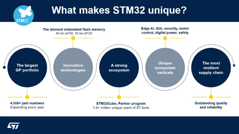
All STM8L low-power products are based on the same architecture with the same memory mapping and a coherent pinout. Additionally, STMicroelectronics and Tapko Technologies have released a KNX communication stack for all ST’s STM8 and STM32 microcontrollers. This initiative will speed up development of smart-building systems for automatic lighting, heating, and other environmental controls that help enhance energy efficiency and user comfort.
Linking to a transceiver
The KNX stack running on a microcontroller can also be used with transceivers such as Silicon Labs’ Si4430/31/32 devices. These are highly-integrated, single-chip, wireless ISM transceivers that allow the RF system designer to choose the optimal wireless part for the application. The Si4430/31/32 are ISM wireless transceivers with continuous frequency tuning over their specified bands, which range from 240–960 MHz and are supported by KNX. The wide operating voltage range of 1.8–3.6 V and low current consumption makes them suitable battery-powered and energy-harvesting applications.

Figure 5: The Si4430/31/32 wireless transceiver.
The integration in the Si4430 offers reduced BOM cost while simplifying the overall system design alongside a low-cost microcontroller. The extremely-low receive sensitivity (–121 dBm) coupled with industry-leading +20 dBm output power ensures extended range and improved link performance. Built-in antenna diversity and support for frequency hopping can be used to further extend range and enhance performance.
The Si4430 family offers advanced radio features including continuous frequency coverage from 240–960 MHz in 156 Hz or 312 Hz steps, allowing precise tuning control along with features such as an automatic wake-up timer, low-battery detector, 64-byte TX/RX FIFOs, automatic packet handling, and preamble detection. All of these reduce the overall current consumption and allow the use of lower-cost 8- or 32-bit system MCUs running the KNX stack from a solar panel. An integrated temperature sensor, general purpose ADC, power on-reset (POR), and GPIOs further reduce overall system cost and size.
The digital receive architecture features a high-performance ADC and DSP-based modem, which performs demodulation, filtering, and packet handling for increased flexibility and performance, although the KNX packet handling has to be implemented by the external microcontroller. The direct digital-transmit modulation and automatic-PA power ramping ensure precise transmit modulation and reduced spectral spreading, ensuring compliance with global regulations including FCC, ETSI, ARIB, and 802.15.4d regulations.
The transceiver uses time division duplexing (TDD), alternately transmitting and receiving data packets, and this approach has to be taken into account in the connection to the microcontroller. The device uses a single-conversion mixer to downconvert the 2-level FSK/GFSK/OOK modulated receive signal to a low IF frequency. Following a programmable gain amplifier (PGA), the signal is converted to the digital domain by an ADC allowing filtering, demodulation, and slicing to be performed in the built-in DSP, increasing the receiver’s performance and flexibility. The demodulated signal is then output to the system MCU through a programmable GPIO or via the standard SPI bus by reading the 64-byte RX FIFO.

Figure 6: Interfacing the Si4430 to a microcontroller to handle the KNX stack.
A single high-precision local oscillator (LO) is used for both transmit and receive modes since the transmitter and receiver do not operate at the same time. The LO is generated by an integrated VCO and Fractional-N PLL synthesizer. The synthesizer is designed to support configurable data rates, output frequency, and frequency deviation at any frequency between 240–960 MHz. The transmit FSK data is modulated directly into the data stream and can be shaped by a Gaussian low-pass filter to reduce unwanted spectral content.
The Si4432’s PA output power can be configured between +1 and +20 dBm in 3 dB steps, while the Si4430/31's PA output power can be configured between –8 and +13 dBm in 3 dB steps. The PA is single-ended to allow for easy antenna matching and low BOM cost. It also incorporates automatic ramp-up and ramp-down control to reduce unwanted spectral spreading. The +20 dBm power amplifier of the Si4432 can also be used to compensate for the reduced performance of a lower-cost, lower-performance antenna or an antenna with size constraints due to a small form-factor, both important factors in linking-up small units such as lighting.
The Si4430/31/32 is designed to work with a microcontroller, crystal, and a few external components to create a very-low-cost system as shown in Figure 6. Voltage regulators are integrated on-chip, which allows for a wide-operating supply voltage range from +1.8 to +3.6 V. A standard 4-pin SPI bus is used to communicate with the external microcontroller running the KNX stack, and three configurable general-purpose I/Os are available. The application in Figure 6 is designed for a system with a TX/RX direct-tie configuration without the use of a TX/RX switch for lower-power smart-home network applications that will use this configuration.
Conclusion
The combination of an open, simplified protocol and low-power, highly-integrated RF transceivers and microcontrollers is opening up new possibilities for the developers of networked equipment for the smart home. Using the lower-frequency bands and the KNX protocol is allowing designs to reach power levels where solar power and other energy-harvesting technologies become possible. This simplifies the installation and maintenance of the smart-home network and helps drive acceptance by the consumer.


