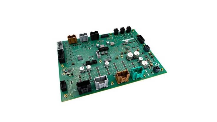
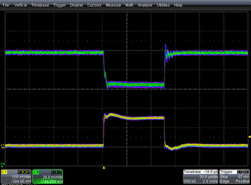
Building high-speed systems using GaN FETs is not a simple matter. Switching electric fields can occupy space above and around the package, so how a system using GaN FETs for wireless systems is assembled is critical for the overall performance. This article looks at the implications of different packaging techniques for different applications and how these can be used to build high performance GaN equipment.
Gallium nitride is rapidly taking over as the technology of choice for certain wireless applications. In areas such as two-way private radio, broadband amplifiers and cellular infrastructure, the advantages of GaN are allowing smaller, more rugged and reliable systems.
When built on a substrate of silicon carbide (SiC), GaN offers higher breakdown voltages than other technologies (over 100 V), as well as electron mobility ten times that of silicon. It is this combination of being able to run at higher temperatures that supports the use in both high-voltage, power switching devices and in RF power amplifiers. With operating channel temperatures over 150°C and a higher power density of 5 to 30 W/mm, class A and AB linear amplifiers are being increasingly used for OFDM, W-CDMA, EDGE and CDMA systems. The higher frequency and power performance means that the devices can be operated at more efficient levels to achieve the same results, giving significant savings in power consumption.

Figure 1: GaN vs. other technologies (source: RFMD).
The world’s cellular network is estimated to consume more than 100 TWh of electricity per year worth roughly $12 billion, and 50 to 80 percent of the networks’ power is consumed by the systems’ power amplifiers and feed infrastructure. Using GaN technology, radio base-station power amplifiers have demonstrated performance improvements of more than 20 percent over incumbent technology at 2.6 GHz operating under the latest 4G LTE signals. This increased power amplifier efficiency could save an estimated 10 TWh per year, the equivalent power output of two nuclear power plants.
While operational cost savings from increased efficiency can be significant, additional substantial savings are also possible in the acquisition cost of the system. A higher-efficiency power amplifier can help OEMs save capital equipment costs through simplified cooling, and the higher-voltage GaN components can lower the cost of AC-to-DC and DC-to-DC converters. Overall, the impact on the total bill of materials can be as much as 10 percent, leading to significantly lower system costs.
Several tier-one telecom OEMs have already incorporated lower-voltage versions of the technology, saving as much as 2,400 MWh of energy.
Cree’s GaN HEMT transistors, such as the CGHV27100 operating at 100 W or 200 W output powers, support both the 1.8 to 2.2 GHz and 2.5 to 2.7 GHz frequency bands. The devices are internally matched for optimum performance, enabling wide instantaneous bandwidths and so are aimed at use in high-efficiency Doherty power amplifiers (PA) where power gains over 18 dB at 2.14 GHz and 16 dB at 2.6 GHz can be achieved.
The high load impedance and low capacitance of the GaN transistor means minimal amount of matching and phase shifting is needed, simplifying the design of a Doherty PA. The high power density leaves plenty of physical space for the design, which, even if not fully optimized, benefits from the raw performance.
The transistor is input matched and supplied in a ceramic/metal pill and flange packages (see Figure 2).

Figure 2: The CGHV27100 GaN HEMT transistor mounted on its evaluation board.
The CGHV27100 supports 2.5 - 2.7 GHz operation with an 18.0 dB gain and 33% efficiency at 25 W. The higher performance of the devices means that a high degree of digital pre-distortion (DPD) correction can be applied.
Digital pre-distortion
The PA consumes more electrical power than any other block in a cellular base station, making it a significant factor in the operating expense for the service provider. The complex digital modulation involved in the wireless protocols means that the PA should be driven well below saturation where it is most efficient. To improve PA efficiency, digital techniques can be used on the signal to reduce the crest factor and improve PA linearity, allowing it to run closer to saturation and reduce power.
Tests have shown 40% efficiency for a typical class AB power amplifier module using DPD, which is a significant improvement over the 10% efficiency of a PA that does not use digital pre-distortion. Having a GaN transistor in the PA allows the amplifier to run at even higher efficiency rates when using DPD, saving millions of dollars a year in a typical network deployment.
For unmatched applications, Cree’s CGH40006S GaN HEMT transistor operates from a 28 Volt rail for general purpose, broadband designs in a variety of RF and microwave applications. GaN HEMTs offer high efficiency, high gain and wide bandwidth capabilities making the CGH40006S ideal for linear and compressed amplifier circuits. The transistor is available in a 3 mm x 3 mm, surface mount, quad-flat-no-lead (QFN) package and supports up to 6 GHz operation with a 13 dB small signal gain at 2.0 GHz and an 11 dB small signal gain at 6.0 GHz.
Assembly
However, building high-speed systems using GaN FETs is not a simple matter. Switching electric fields can occupy space above and around the package, coupled with the higher power through the packaging, means the assembly of a wireless system using GaN FETs is critical for the overall performance.
The ultra-high-speed switching capabilities of GaN FETs enable a new state-of-the-art in power density. To achieve these switching speeds requires minimal inductance to reduce dynamic losses and ringing which is not possible with traditional packaging approaches. EPC’s innovative wafer level, Land Grid Array (LGA) packaging enables high frequency loop inductance of a half bridge circuit to be demonstrated as low as 400 pH, which allows overshoot of just 23%, minimal ringing, and a 2.5% efficiency gain compared with a 1.6 nH layout at 12 V, 1 MHz.

Figure 3: The mounting side of a GaN FET that has a land pitch of 0.4 mm.
With these new packages, the assembly process for such devices is more stringent as well. For a reliable, high yielding assembly, LGA eGaN FETs must have all flux rinsed from between lands, be dry before applying power, and be assembled level to the board with enough standoff to rinse any flux from between the lands.
This also means the correct solder volume and reflow process is needed to provide sufficient height for proper rinsing of any solder flux from between the lands, but not excessive solder, where the joint becomes unstable and tilts or collapses during reflow. Here the correct PCB solder mask footprint for each solder bump ensures proper containment of the solder.
The LGA footprint is solder mask defined. This means that the copper trace is larger than the solder mask opening in all directions, bounding the solder flow by the solder mask. Solder mask openings should be slightly smaller than the corresponding solder bump. Oversized solder mask openings can lead to solder bridging from land to land in the short direction, too narrow a channel for sufficient rinsing, or die tilt in the long direction. Undersized openings lead to solder overflowing the solder mask causing shorts or die tilt. This is especially critical for small bumps when larger bumps are also present on the die, and the typical solder mask thickness should not exceed 25 μm.
While the eGaN FET LGA package is quite small, these devices are designed to carry significant current and this impacts on the design of the copper trace. Heavier copper traces may become too narrow for the 0.4 mm pitch while lighter traces will sacrifice thermal and electrical performance. Vias also should not be placed in the lands unless they are completely filled, as unfilled vias will wick solder away from the joint and this again may cause die tilt or insufficient standoff for proper cleaning.
Solder volume and stencil design
Correct solder volume will help ensure a proper assembly and allow proper cleaning of the device which is essential in delivering reliable equipment. For type 3 solder, reflowed solder volume from the paste should be roughly equal to the solder volume on each terminal above the solder mask. Care must be taken to account for the metal load of the solder when determining the solder volume in the solder mask and stencil opening areas and the volume will be based on stencil thickness, ideally 100 μm.
Type 4 solder has smaller particles, and flows more freely leading to a higher risk of die tilt and solder bridging. If type 4 solder must be used, less solder is required. For example, the 180 μm wide stencil opening for the EPC2001 should be reduced to 165 μm for type 4 solder.
For a 100 μm stencil, type 3 solder, 88.5% metal loading, the stencil opening should be the same size as the solder mask opening with the corners of the apertures rounded to a radius of 60 μm.
Laser cut stencils have a straighter wall than chemically etched stencils and so will, in general, result in more solder volume released than a chemically etched stencil of the same aperture. The 180 μm wide stencil aperture is recommended for a laser cut stencil. A slight adjustment wider (up to 200 μm wide) might be required for chemically etched stencils to obtain sufficient solder volume release.
Underfill
Underfill should be used in applications where the board is exposed to moisture that may provide an environment, which allows dendrite growth. Incomplete cleaning and drying can leave uncured flux, which is a medium in which dendrites can grow.
A tilted die will make the device impossible to thoroughly clean, leaving residual flux and enabling dendrite growth. The main causes of die tilt were found to be uneven thickness of solder paste, excessive vibration during reflow, non-optimized temperature profile and oversized solder mask and/or oversized solder stencil from a solder volume that is too high. Normally, the solder flows evenly and melts roughly at the same time. Care must be taken to adjust the solder reflow profile when an element of significant mass is located nearby. All of the solder has to flow for the surface tension to level and align the device.
Solder bridging can occur due to excessive solder volume or undersized solder mask opening, particularly where bump lengths vary within a die such as the gate and substrate bumps of the EPC2001. The excess volume does not have enough surface tension to hold the solder together, and the solder collapses, shorting one terminal to another. Too wide a solder mask opening can reduce the distance between the solder between bars and make it easier to short.
Conclusion
LGA packages provide the low inductance necessary to take full advantage of the ultra-fast switching capabilities of GaN FET technology. With proper manufacturing techniques, assemblies using GaN FETs will have high yield and a long, reliable working life.
The LGA device footprint is solder mask defined, so the mask designs should be according to the recommended land pattern on the datasheet. Correct solder volume and reflow profile will help ensure mounted die are level with enough standoff for proper rinsing. Rinsing in all directions and drying are required to remove residue that would otherwise enable dendrite growth.
The reflow temperature profile must be adjusted to ensure complete reflow and to help avoid the die tilt that causes flux to be trapped and allows dendrites to grow.
This combination of new packaging and higher performance devices is helping to save millions of dollars in operating costs for network operators. Using the higher performance of the GaN devices to support more digital pre-distortion allows the power amplifiers to operate more efficiently, saving significant amounts of power. Using new types of robust packaging, with attention paid to the assembly of the systems, allows these designs to be more reliable and even more effective.


