

Intel公司的Stratix 10 GXFPGA和SX SoC系列产品比前一代产品成本提供2X性能和高达70低功耗,具有几个开创性的创新如所有新型HyperFlex™和架构,能满足日益增长的带宽和处理性能,而满足功率预算.嵌入硬件系统基于四核64位ARM®Cortex®-A53,采用Intel 14-nm Tri-Gate (FinFET)技术和混合性3D片上系统(SiP)技术,单片核多达550万和逻辑单元,多达96个全双工收发器,数据速率高达28.3Gbps,主要用在计算和存储,网络设备,光传输网络,广播,军用雷达,医疗设备,测试和测量以及5G无线设备,ASIC原型.本文介绍了Intel StraTIx 10 GXFPGA和SoC器件主要特性,架构框图以及Intel® StraTIx® 10 GX FPGA 开发板主要特性和详细电路图.
Intel’s 14-nm Intel® StraTIx® 10 GX FPGAs and SX SoCs deliver 2X the coreperformance and up to 70% lower power over previous generaTIon high-performanceFPGAs.Featuring several groundbreaking innovations, including the all new HyperFlex™ core architecture, this device family enables you to meet the demand for ever-increasing bandwidth and processing performance in your most advanced applications, while meeting your power budget.
With an embedded hard processor system (HPS) based on a quad-core 64-bit ARM® Cortex®-A53, the Intel Stratix 10 SoC devices deliver power efficient,application-class processing and allow designers to extend hardware virtualization into the FPGA fabric. Intel Stratix 10 SoC devices demonstrate Intel’s commitment to high-performance SoCs and extend Intel’s leadership in programmable devices featuring an ARM-based processor system.
Important innovations in Intel Stratix 10 FPGAs and SoCs include:
• All new HyperFlex core architecture delivering 2X the core performance comparedto previous generation high-performance FPGAs
• Industry leading Intel 14-nm Tri-Gate (FinFET) technology
• Heterogeneous 3D System-in-Package (SiP) technology
• Monolithic core fabric with up to 5.5 million logic elements (LEs)
• Up to 96 full duplex transceiver channels on heterogeneous 3D SiP transceivertiles
• Transceiver data rates up to 28.3 Gbps chip-to-chip/module and backplaneperformance
• M20K (20 kbit) internal SRAM memory blocks
• Fractional synthesis and ultra-low jitter LC tank based transmit phase locked loops(PLLs)
• Hard PCI Express® Gen3 x16 intellectual property (IP) blocks
• Hard 10GBASE-KR/40GBASE-KR4 Forward Error Correction (FEC) in everytransceiver channel
• Hard memory controllers and PHY supporting DDR4 rates up to 2666 Mbps per pin
• Hard fixed-point and IEEE 754 compliant hard floating-point variable precisiondigital signal processing (DSP) blocks with up to 10 TFLOPS compute performancewith a power efficiency of 80 GFLOPS per Watt
• Quad-core 64-bit ARM Cortex-A53 embedded processor running up to 1.5 GHz inSoC family variants
• Programmable clock tree synthesis for flexible, low power, low skew clock trees
• Dedicated secure device manager (SDM) for:
— Enhanced device configuration and security
— AES-256, SHA-256/384 and ECDSA-256/384 encrypt/decrypt accelerators and
authentication
— Multi-factor authentication
— Physically Unclonable Function (PUF) service and software programmabledevice configuration capability
• Comprehensive set of advanced power saving features delivering up to 70% lowerpower compared to previous generation high-performance FPGAs
• Non-destructive register state readback and writeback, to support ASICprototyping and other applications.
With these capabilities, Intel Stratix 10 FPGAs and SoCs are ideally suited for the most demanding applications in diverse markets such as:
• Compute and Storage—for custom servers, cloud computing and data centeracceleration
• Networking—for Terabit, 400G and multi-100G bridging, aggregation, packetprocessing and traffic management
• Optical Transport Networks—for OTU4, 2xOTU4, 4xOTU4
• Broadcast—for high-end studio distribution, headend encoding/decoding, edgequadrature amplitude modulation (QAM)
• Military—for radar, electronic warfare, and secure communications
• Medical—for diagnostic scanners and diagnostic imaging
• Test and Measurement—for protocol and application testers
• Wireless—for next-generation 5G networks
• ASIC Prototyping—for designs that require the largest monolithic FPGA fabricwith the highest I/O count
Intel Stratix 10 GXFPGA和SoC器件主要特性:


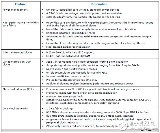
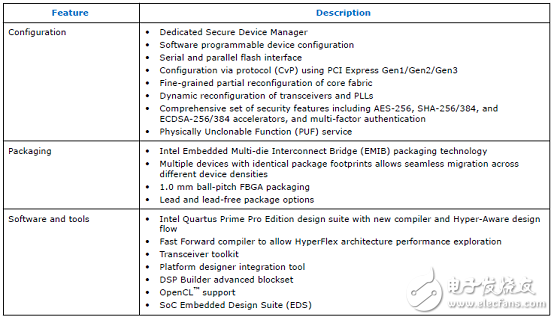
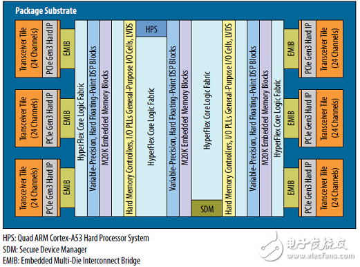
图1.Intel Stratix 10 GXFPGA和SoC架构框图
Intel® Stratix® 10 GX FPGA 开发板
The new Intel Quartus® Prime Design Suite design software includes everythingneeded to design for Intel FPGAs, SoCs and CPLDs from design entry and synthesis tooptimization, verification and simulation. The Intel Quartus Prime Design Suitesoftware includes an additional Spectra-Q® engine that is optimized for future devices.
The Spectra-Q engine enables new levels of design productivity for next generation programmable devices with a set of faster and more scalable algorithms, a hierarchical database infrastructure and a unified compiler technology.
The Intel Quartus Prime Design Suite software is available in three editions based on specific design requirements: Pro, Standard, and Lite Edition. The Intel Stratix 10FPGA Development Kit is supported by the Intel Quartus Prime Pro Edition.
Intel Quartus Prime Pro Edition: The Intel Quartus Prime Pro Edition is optimized tosupport the advanced features in Intel’s next generation FPGAs and SoCs, startingwith the Intel Arria® 10 device family and requires a paid license.
Included in the Intel Quartus Prime Pro Edition are the Intel Quartus Prime software,Nios® II EDS and the MegaCore IP Library. To install Intel’s development tools,download the Intel Quartus Prime Pro Edition software from the Intel Quartus PrimePro Edition page in the Download Center of Intel’s website.

图2.Intel® Stratix® 10 GX FPGA 开发板外形图(正面)
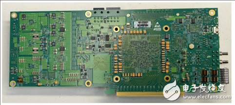
图3.Intel® Stratix® 10 GX FPGA 开发板外形图(背面)
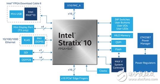
图4.Intel® Stratix® 10 GX FPGA 开发板框图
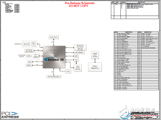
图5.Intel® Stratix® 10 GX FPGA开发板电路图(1)
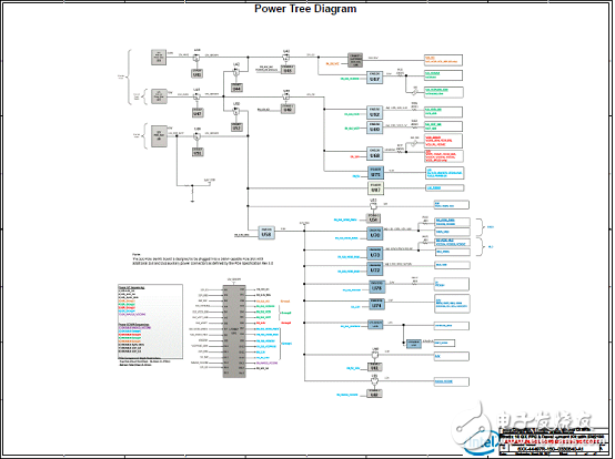
图6.Intel® Stratix® 10 GX FPGA开发板电路图(2)

图7.Intel® Stratix® 10 GX FPGA开发板电路图(3)
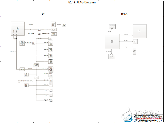
图8.Intel® Stratix® 10 GX FPGA开发板电路图(4)

图9.Intel® Stratix® 10 GX FPGA开发板电路图(5)
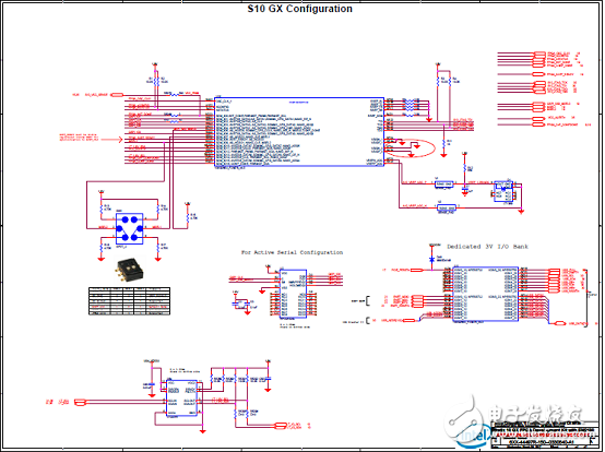
图10.Intel® Stratix® 10 GX FPGA开发板电路图(6)
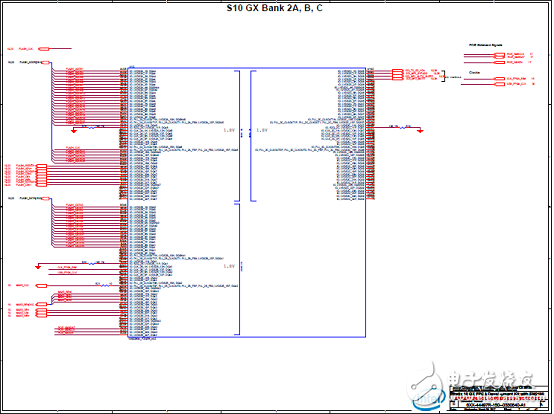
图11.Intel® Stratix® 10 GX FPGA开发板电路图(7)

图12.Intel® Stratix® 10 GX FPGA开发板电路图(8)

图13.Intel® Stratix® 10 GX FPGA开发板电路图(9)

图14.Intel® Stratix® 10 GX FPGA开发板电路图(10)

图15.Intel® Stratix® 10 GX FPGA开发板电路图(11)

图16.Intel® Stratix® 10 GX FPGA开发板电路图(12)
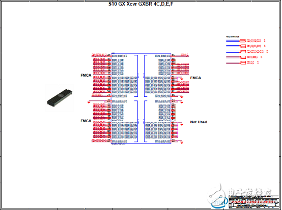
图17.Intel® Stratix® 10 GX FPGA开发板电路图(13)
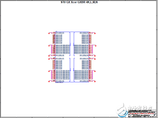
图18.Intel® Stratix® 10 GX FPGA开发板电路图(14)
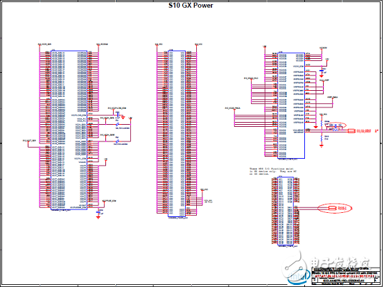
图19.Intel® Stratix® 10 GX FPGA开发板电路图(15)

图20.Intel® Stratix® 10 GX FPGA开发板电路图(16)
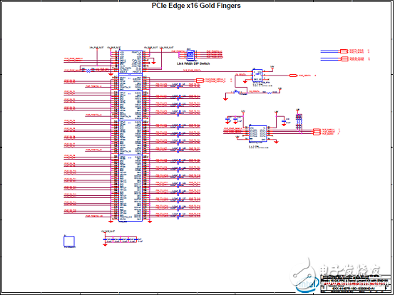
图21.Intel® Stratix® 10 GX FPGA开发板电路图(17)

图22.Intel® Stratix® 10 GX FPGA开发板电路图(18)
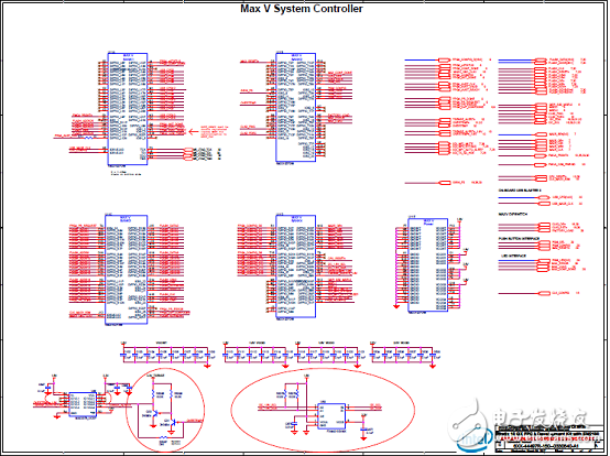
图23.Intel® Stratix® 10 GX FPGA开发板电路图(19)
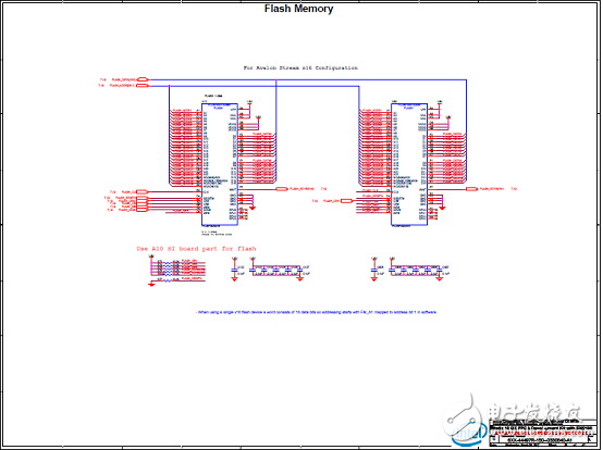
图24.Intel® Stratix® 10 GX FPGA开发板电路图(20)

图25.Intel® Stratix® 10 GX FPGA开发板电路图(21)

图26.Intel® Stratix® 10 GX FPGA开发板电路图(22)
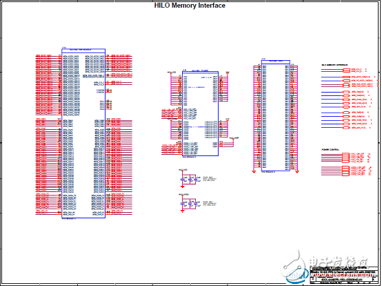
图27.Intel® Stratix® 10 GX FPGA开发板电路图(23)
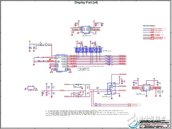
图28.Intel® Stratix® 10 GX FPGA开发板电路图(24)
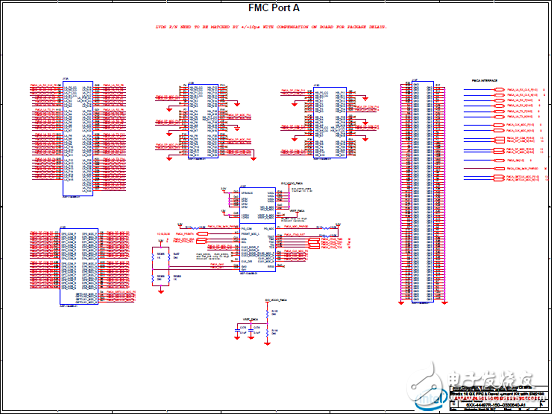
图29.Intel® Stratix® 10 GX FPGA开发板电路图(25)

图30.Intel® Stratix® 10 GX FPGA开发板电路图(26)
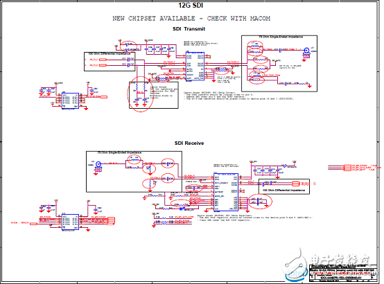
图31.Intel® Stratix® 10 GX FPGA开发板电路图(27)

图32.Intel® Stratix® 10 GX FPGA开发板电路图(28)

图33.Intel® Stratix® 10 GX FPGA开发板电路图(29)

图34.Intel® Stratix® 10 GX FPGA开发板电路图(30)

图35.Intel® Stratix® 10 GX FPGA开发板电路图(31)

图36.Intel® Stratix® 10 GX FPGA开发板电路图(32)
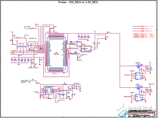
图37.Intel® Stratix® 10 GX FPGA开发板电路图(33)
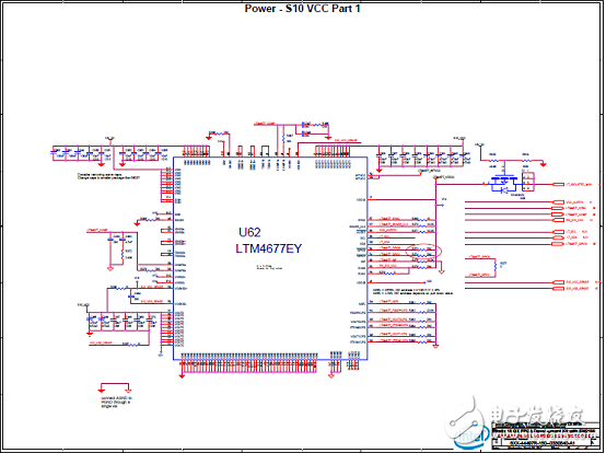
图38.Intel® Stratix® 10 GX FPGA开发板电路图(34)

图39.Intel® Stratix® 10 GX FPGA开发板电路图(35)
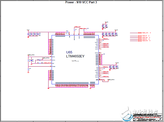
图40.Intel® Stratix® 10 GX FPGA开发板电路图(36)
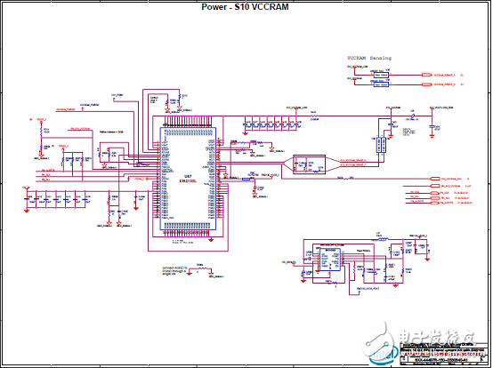
图41.Intel® Stratix® 10 GX FPGA开发板电路图(37)
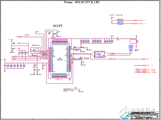
图42.Intel® Stratix® 10 GX FPGA开发板电路图(38)
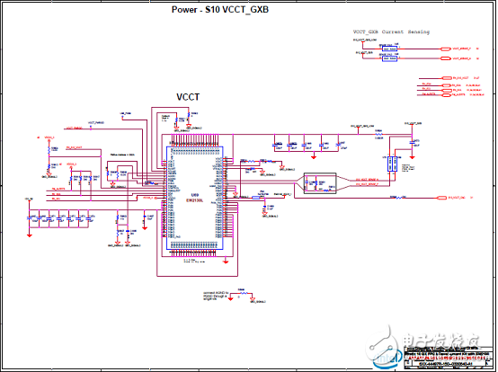
图43.Intel® Stratix® 10 GX FPGA开发板电路图(39)
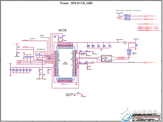
图44.Intel® Stratix® 10 GX FPGA开发板电路图(40)
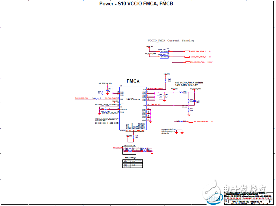
图45.Intel® Stratix® 10 GX FPGA开发板电路图(41)
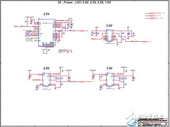
图46.Intel® Stratix® 10 GX FPGA开发板电路图(42)

图47.Intel® Stratix® 10 GX FPGA开发板电路图(43)

图48.Intel® Stratix® 10 GX FPGA开发板电路图(44)
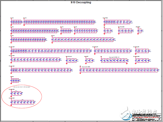
图49.Intel® Stratix® 10 GX FPGA开发板电路图(45)
图50.Intel® Stratix® 10 GX FPGA开发板电路图(46)